AuSn / Pb Free Solders
Gold-tin solder alloys, with compositions ranging from the eutectic 80/20 Au/Sn to 73/27, are used for integrated circuit chip or die bonding, because of their high bond strength, adhesion, resistance to creep, low stress, corrosion resistance, good thermal conductivity and absence of whisker formation. Solder preforms are costly, and become difficult to use as required sizes shrink. Solder pastes can have both process capability issues and shortcomings in high performance device reliability and durability.
JVD™ thin film AuSn solder layers offer a manufacturable solution.
We use the JVD process to deposit eutectic AuSn solder layers with thicknesses typically from 1 to 10 microns, and have deposited over 20 microns. Alloy composition is precisely maintained from source to substrate as we deposit the alloy; our process does not deposit alternating Au and Sn layers. Metal capture efficiency can exceed 90% with little waste of expensive metal. We do batch or single part processing depending on the substrate, and can handle round wafers, ceramic squares and rectangles, Si and III-V wafers in sizes ranging from 2" to 8", down to the smallest submounts and heatsinks in custom holders. Patterned photoresists remain cool during our process with the vast majority of jobs not exceeding 120 degrees C.
We have the ability to deposit up to 4 different materials in a single run using JVD sources. For example, we can deposit adhesion / diffusion barrier / AuSn / Au layers in a continuous sequence without breaking vacuum.
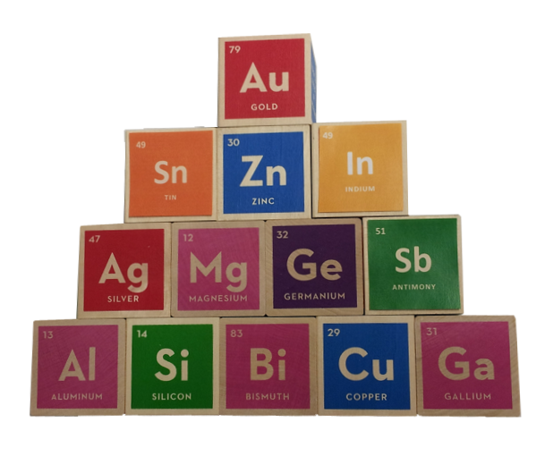
Lead free soldering has become a primary goal in advanced microelectronics, semiconductor packaging and related worldwide markets. We can deposit many of the elements of greatest importance in lead free solder such as Au, Ag, Sn, Cu, singly or in alloy form, with excellent control over alloy composition.
We can deposit solder bumps of extremely small size and high area density by high rate deposition of AuSn through patterned photoresist with feature sizes below 10 microns, e.g.: 4 X 4 microns with 8 micron pitch.
Related information on JVD advantages and capabilities for lead free solder deposition can be found in the Technology - JVD™ Processes section.
For additional information click here for the February 2003 article on JVD gold-tin solder in Advanced Packaging magazine.
For more information on offerings and pricing, please contact us.