JVD™ Technology
Home / About Us
JVD™ Technology
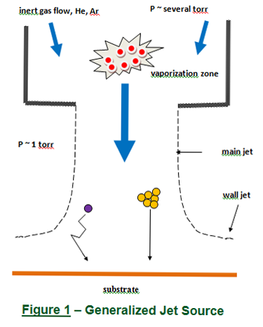
JVD’s main innovation is a novel vapor source: a sonic jet of inert gas in “low” vacuum, ~ 1 torr pressure that transports condensable atoms, molecules, or clusters from a nozzle to a substrate. The jet deposits these species efficiently in a small area, less than the size of a dime. Larger areas, an 8″ wafer for example, are coated by imposing a relative 2D motion between substrates and one or more jet sources. This combination of jet sources and relative motion gives JVD great versatility.
We have designed a number of jet sources based on different vaporization mechanisms inside the nozzle as illustrated in Figure 1. Ultra high purity Helium or Argon is supplied to the nozzle and exits from it as a jet. Ordinarily, the nozzle pressure is several torr, and the downstream pressure is a torr or less, but the range is wide; in different applications both pressures can be higher or lower. This high purity, high speed gas flow is driven only by mechanical pumps and blowers, a robust technology with fast startup times.

These jet sources are the basis of multiple jet, moving substrate processes for depositing metals, semiconductors, dielectrics, and organics, as well as oxides and nitrides in a “reactive” mode. All these materials can be grown by JVD in different forms: “atomistic” or “nanocluster”, multiple-layers, multi-component alloys, and “host-guest” films. In addition to solder deposition, JVD’s range of materials and applications are reviewed in Chapter 18 of the Handbook of Deposition Technologies for Films and Coatings, Third Edition, edited by Peter M. Martin.
Solder Deposition in JVD
Solder alloys of precise composition are available commercially as wire or ribbon, and these form the starting materials for the “wire feed” jet source. The wire-feed is JPC’s mainstay for commercial production of solder coatings; as an example, consider AuSn. A fine wire or ribbon of AuSn alloy is fed against a hot W coil located upstream of the nozzle exit. On contact, the AuSn wire melts, wets, and vaporizes; individual Au and Sn atoms are swept downstream with the jet and deposit on the substrate, concentrated within a circle ~ 1 cm in diameter; radial diffusion of Au and Sn in the jet gives the AuSn deposit a Gaussian profile. At constant AuSn wire feed rate the flux of Au and Sn atoms is also constant, and the AuSn deposition rate is proportional to wire feed rate; this considerably simplifies thickness calibration. The Au to Sn ratio of the wire is preserved in the growing film, a critical consideration for solder bumping.
Pre-cleaning is possible by including a second hot filament for thermionic emission of electrons; this “e-jet” configuration ignites a low voltage, high-current Argon plasma jet. Low energy Ar+ ions in the jet then bombard and gently clean the substrate.
The wire feed can be used for metals that do not alloy with and degrade the hot tungsten coil structure. This includes all metals and alloys commonly used for solder deposition, such as AuSn, InSn, and SnAg. Very high rates are possible with this wire feed jet source; even a relatively slow wire feed can give deposition rates approaching microns per minute over a 4″ wafer. Most of JPC’s commercial deposition of solders is carried out with the hot filament wire feed / e-jet combination, both in atomistic and cluster modes.
For the much thinner adhesion/diffusion barrier layers, such as Ti and Pt, we have used for many years a jet source based on hollow cathode sputtering at “high” pressures of ~ 1 torr. A hollow cathode provides a target for Argon glow discharge sputtering of metal atoms, and also plays the role of a cylindrical nozzle. Argon is let in at one end, flows through the hollow cathode, and forms the sonic jet which sweeps sputtered atoms to the substrate. JVD sputter jet sources give much lower deposition rate than the wire feed, but they can generate metal vapor, and are appropriate for thin films of Ti, Pt, and Au required as adhesion, diffusion barrier, and protective layers prior to solder bumping. The deposition rate can be calibrated against Ar+ sputter current; when the gas flow conditions are fixed, this calibration is stable and accurate.
